Journal of Fuzzy Systems and Control, Vol. 2, No 1, 2024 |
Enhancement of the Properties of Solar Cells Fabricated by Cadmium Oxide Deposited on Porous Silicon
Raghad R. Mahdi 1,*, Samier A. Maki 2, Hind A. AL Salihi 3, Marwa K. Abood 4, Raghad J. Halbos 5,
Ruqia Abdulhussien Hassan 6, M. A. Fayad 7
1,3,5,6,7 Energy and Renewable Energies Technology Center, University of Technology- Iraq, Baghdad, Iraq
2 Applied Science College, University of Baghdad, Iraq
4 Applied Science Department, University of Technology- Iraq, Baghdad, Iraq
Email: 1 raghad.r.mahdi@uotechnology.edu.iq, 3 hind.a.mahdi@uotechnology.edu.iq, 4 marwa.k.abood@uotechnology.edu.iq, 5 raghad.j.halbos@uotechnology.edu.iq, 6 ruqia.a.hassan@uotechnology.edu.iq, 7 mohammed.a.fayad@uotechnology.edu.iq
*Corresponding Author
Abstract—This work describes the synthesis of cadmium oxide by a straightforward chemical process and its deposition onto a porous silicon substrate using the drop-casting technique. X-ray diffraction was utilized to determine the structure of the produced cadmium oxide (CdO). The results indicated that the CdO synthesized at room temperature is a cubic polycrystalline structure with a peak at 111. The grain size of the CdO exhibits a high level of homogeneity. The mean roughness of the produced CdO thin film was demonstrated using atomic force microscopy (AFM). The study utilized the optical properties of CdO, revealing its strong absorption and low transmission characteristics. A solar cell was created by depositing cadmium oxide onto prepared porous silicon to verify its high conversion efficiency of approximately 5.8%. The study examines the physical characteristics and effectiveness of a solar cell constructed using cadmium oxide placed on porous silicon.
Keywords—Cadmium Oxide; X-Ray; Solar Cell; Porous Silicon; Fabricated; Homogenous
This research generally focuses on the production of solar cells as the process of converting light energy into electricity. Cadmium oxide cells are a technology in which a thin layer of cadmium oxide conducts electricity to collect light and turn it into power. Cadmium oxide is produced in many ways, one of which involves preparing a glass or silicon surface as a base for the cell and subsequently depositing the material on top of these bases. Various procedures and technologies are used to apply a coating of semi-conducting materials like silicon to cadmium oxide to enhance its characteristics and boost its conversion efficiency [1]-[3].
Cadmium oxide is a naturally occurring n-type semiconductor material with a cubic and faceted crystalline structure. It has an energy gap ranging between 2.16 and 2.6 eV, an index of refraction of 2.7, and a molar mass of 128.2 g/mol [4]-[8]. Cadmium oxide can dissolve in water and is utilized in various applications, including catalysts, gas sensors, solar cells, and optical detectors [9]-[11]. The procedure involves combining various materials until the desired cell material is obtained. Once the material is deposited on silicon bases, it is considered a fundamental component in the production of photoelectric devices due to its various physical and chemical properties, such as a narrow energy gap of 1.12 eV, crystal structure, and diverse colors. The silicon used in this study is prepared using various techniques to enhance its properties. It is utilized in the production of important applications due to its specific response and operation in the red zone, such as emitting devices and detectors [12]-[15].
This work aims to analyze the physical parameters of a solar cell made from cadmium oxide placed on porous silicon and determine the efficiency of this cell.
Cadmium oxide is used in this work as a chemical element by the simple chemical method, which includes mixing many materials in certain quantities to have the required material and then depositing it on a silicon substrate by the drop-casting method. The simple chemical method is considered a fast and low-cost method without the need for complex devices to work.
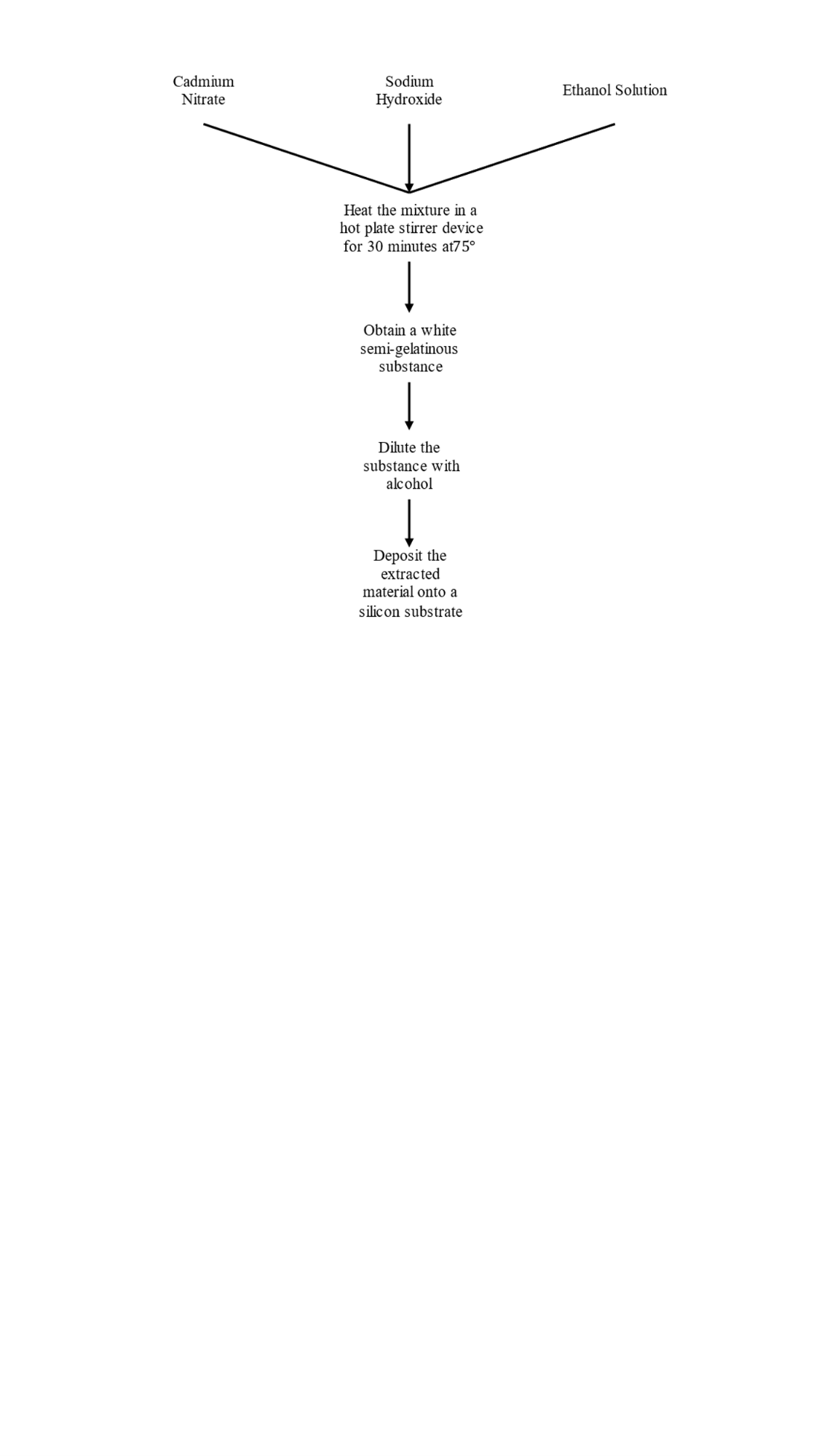
CdO is fabricated by mixing 1.5 g of cadmium nitrate with 1.5 g of sodium hydroxide and 50 mil of ethanol solution with PVC solution to ensure the sticks to the silicon substrate. The solution is heated in a hit-and-stirrer device for half an hour at 75 °C. After the heating process, the final product is a white semi-gelatinous substance, which is then diluted with alcohol in order for the heavy material to lie down and the required material to settle to the top to be pulled by a special syringe (YE3k061872:10–100 ML).
The final product is deposited on the glass by the drop-casting method, where one drop is placed in a special syringe and then heated to dry for 10 minutes. At the end, we noticed that the substance had changed from white to yellow, which is the cadmium oxide material. The flow chart of the preparation process is shown in Fig.1.
Porous silicon is fabricated by using P-type silicon; one of the silicon sides is covered with electrodes, as it is coated with a thick layer of aluminum in the electric evaporation chamber, which starts from pressure (10–5) torr. After the process of electrodeposition, the silicon is cleaned with a solution of Hydrofluoric acid (HF) for 5 minutes and left to dry [14]. After drying, it is cut in the same dimensions for the cell opening, about 1 cm, to avoid the leakage process. The process begins with the use of a highly concentrated solution (Hf) and ethanol 99.9% inside the electric cell at room temperature and a 10 µA/cm2 current density with a 15-s etching time inside the electric cell made of a high-acid-resistant polymer like Teflon. In contrast, the cathode or anodic cell is made of platinum or materials with a conductive resistance, so the porous silicon is ready to drip the prepared CdO on it. All the necessary tests for the CdO thin films made from which the cell is made and study the measurements of the properties (I-V) of the sample prepared inside the dark room by connecting the negative part of the sample to the negative voltage of the continuous power supply (D.C. power supply) of the type (Dazheng; Ps-303D) and connecting the positive part of the sample to the positive voltage of the power supply within a range (0-10)V, in the case of forward bias, the (I-V) are calculated in the dark case for the reverse bias by connecting the negative part of the simple to the positive part of the continuous power supply. Also, the characteristics of the I-V for the prepared sample inside the bright room are obtained by using a white light lamp (halogen lamp) (24V, 50W) manufactured by the Wotan-Germany Company. The reversal bias voltage is variable within the range (0–10) V, and when we obtain the amount of voltage generated in the absence of any external bias voltage by using a Keithily 619 digital electrometer, which is a type of meter, and a box of resistors ranging (1-100) MΩ.
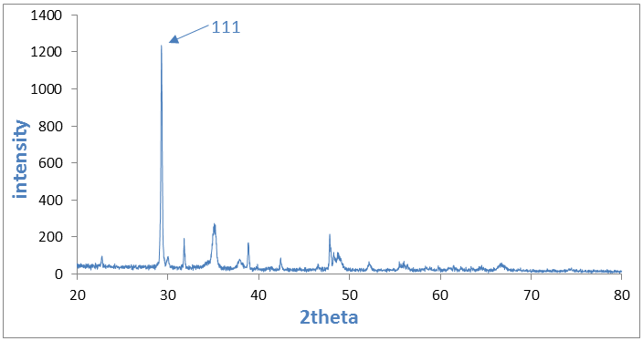
Fig. 2 shows the Xrd patterns of the prepared CdO thin film by the chemical simple method which contains the peak (111) of the CdO at (29 .8) which was compared to the JEPDS card No (03-065-2908). The crystal size (D) and the dislocation density (ᵹ), microstrain (η) values are calculated from the following equations [15]-[19]:
| (1) |
| (2) |
| (3) |
where  is the wavelength used, β is the full FWHM of the peak, Ɵ is the Bragg angle, δ is the density of dislocation, and ε is the stress.
It is found that the greatest intensity was at the angle 2Ф= 29.28, and the dislocation density, the microstrain, and the crystalline size are shown in Table 1.
Sample | 2 Ф | (hkl) | FWHM (deg) | ε *10-4 (lines-2.m-4) | D (nm) | δ Line.m-2 |
As prepared | 29.28 | 111 | 0.159 | 0.674 | 52.37 | 3.7892 |
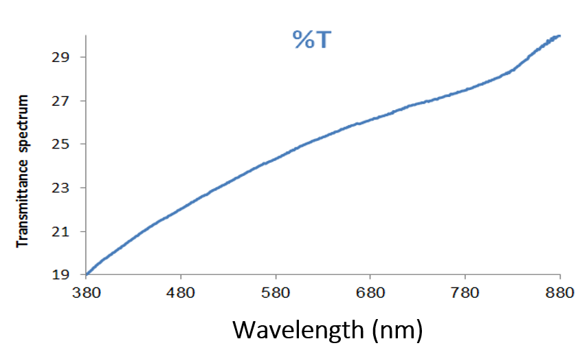
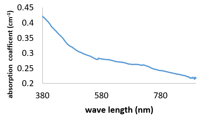
From the study of the optical properties, Fig. 3 and Fig. 4 show the transmittance and absorption spectrum of the CdO films, as it starts to increase from 19 % to a maximum transmittance is 30%.
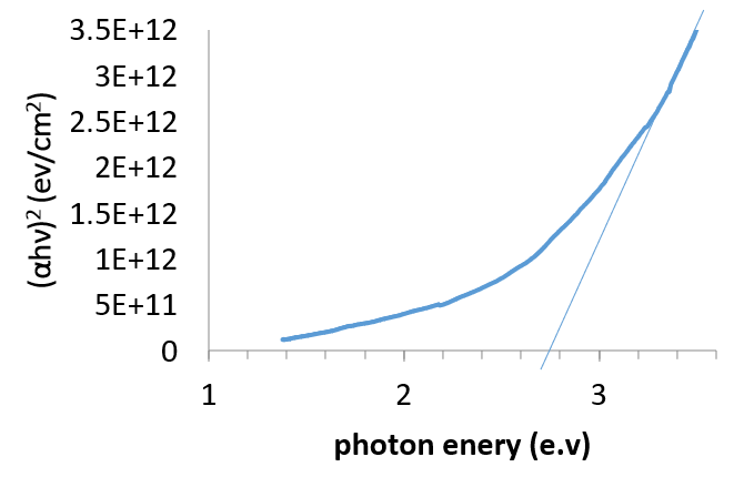
The energy gap value of the prepared film was measured by the extrapolation of the linear parts of The curved plotted between (αhν)2 versus (hν) (Tauc plot), with photon energy giving the value of Eg as shown in Fig. 5.
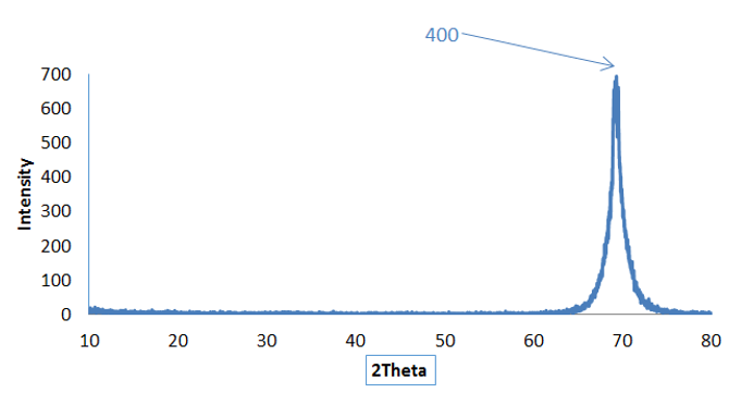
The x-ray diffraction for the prepared porous silicon by etching process is cubic (FCC) and polycrystalline is presented in Fig. 6, which contains the peak (004) at the angle (69.27) which is compared with the basic value set by the Shimadzu 6000. Table 2 shows the structure parameters of the psi.
sample | 2 Ф | (hkl) | FWHM (deg) | ε *10-4 (lines-2.m-4) | D (nm) | δ Line.m-2 |
psi | 69.27 | 004 | 1.299 | 1.0641 | 12690.4 | 6.2093 |
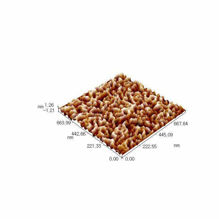
Fig. 7 shows a uniform and homogenous surface with a vertical matrix and spherical shape, separated by nano distance and the RMS value in limit 0.712 nm. The roughness right is in the limit of 0.617 nm, and the averaged diameter is in the limit of 24.08 nm.
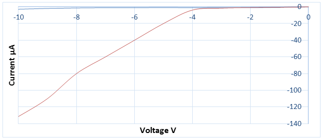
Fig. 8 shows the behavior of the I-V applied to the fabricated cell in both cases of forward and reverse bias, in dark current in the case of forward bias increases with the increase in voltage [20]-[24], as well as in the dark current in the case of the reverse bias.
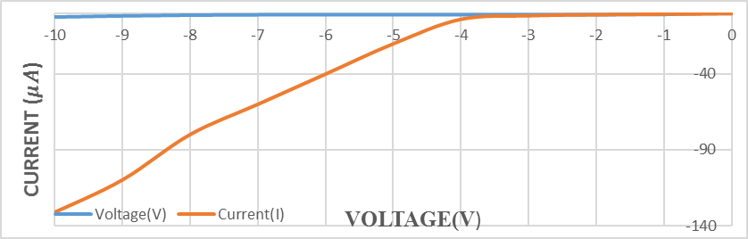
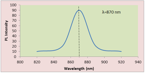
Fig. 9 shows the behavior of the (I-V) in the case of illumination, where the cell is exposed to white light. It can be noticed that the current in reverse bias increases with the increase in the voltage. The characteristics of the prepared solar cell such as full factor (F.F) and the efficiency (η) were measured and illustrated in Table 3. Fig. 10 shows the photoluminescence special studies for the porous silicon (p-type) in current (10) µA and amount of time (15) s. It can be obtained that the largest value of PL appears at the wavelength of 870 nm, so the energy gap is approximately 1.4 ev.
Sample | Imax (μA) | Vmax (V) | Imax (μA) | Vmax (V) | F. F | η % |
As- prepared | 8 | 1.1 | 6.2 | 0.8 | 62 | 5.8 |
The study concluded that a cadmium oxide thin film was successfully prepared using a simple chemical method. The optical properties indicated a decrease in absorption with increasing absorbed photon wavelength, and the energy band gap was measured to be 3.2 eV. The AFM image showed an average grain size of 24 nm, while XRD analysis confirmed the presence of faces-centered cubic (FCC) in the cadmium oxide particles with a grain size of around 52 nm. Porous silicon was fabricated through an etching process inside an electric cell at room temperature. The characteristics of a solar cell were also studied, showing an efficiency of 5.8% in both dark and light conditions.
Raghad R. Mahdi, Enhancement of the Properties of Solar Cells Fabricated by Cadmium Oxide Deposited on Porous Silicon