Journal of Fuzzy Systems and Control, Vol. 2, No 2, 2024 |
|
Study of Some Properties of Solar Cell Fabricated by Depositing Cadmium Oxide on Porous Silicon at Varying Temperatures
Raghad R. Mahdi 1,*, Samier A. Maki 2, Hind A. AL Salihi 3, Marwa K. Abood 4, Raghad J. Halbos 5,
Ruqia Abdulhussien hassan 6, M. A. Fayad 7
1, 3, 5, 6,7 Energy and Renewable Energies Technology Center, University of Technology- Iraq, Baghdad, Iraq
2 Applied Science College, University of Baghdad, Iraq
4 Applied Science Department, University of Technology- Iraq, Baghdad, Iraq
Email: 1 raghad.r.mahdi@uotechnology.edu.iq, 3 hind.a.mahdi@uotechnology.edu.iq, 4 marwa.k.abood@uotechnology.edu.iq, 4 raghad.j.halbos@uotechnology.edu.iq, 5 ruqia.a.hassan@uotechnology.edu.iq, 6 mohammed.a.fayad@uotechnology.edu.iq
*Corresponding Author
Abstract—In this research, cadmium oxide  was prepared by using the simple chemical method, and porous silicon was fabricated by using the etching technique on regular silicon. A solar cell is fabricated by depositing the
  on the prepared porous silicon ( /Psi) by the drop-casting method and doing the annealing process at three different temperatures (200, 400, and 600 °C). The X-ray diffraction analysis tests show that all the prepared samples are polycrystalline and cubic with orientation peaks (111, 101, 100, 102). The optical tests show that these thin films have a high absorbency and low transmittance decrease with increasing the annealing temperature. The short circuit current
  and the short circuit voltage
  of the fabricated solar cell showed that the conversion efficiency increased as the annealing process temperature increased until it reached 9.3% at 600 ˚C.
Keywords—Cadmium Oxide; Deposited; Solar Cell; XRD; Fabricated; Films
Introduction
Cadmium oxide is a type of semiconductor oxide material that belongs to the II-VI group and has n-type conductivity. Cadmium oxide occurs naturally in two forms: crystalline and randomly arranged. The crystalline structure of CdO is cubic, specifically face-centered cubic (FCC) [1]. Cadmium oxide possesses several important characteristics, including a significant energy gap of 2.16-2.6 electron volts [2], a refractive index of 2.75, and a high density of 8150 kilograms per cubic meter [3][4]. Cadmium oxide has multiple applications, such as in solar cells [5], phototransistors, catalysts, transparent electrodes, gas sensors [6], photodiodes, and optoelectronic devices. Cadmium oxide thin films are fabricated by several techniques, such as sol-gel, sequential ionic layer adsorption and reaction (SILAR), pulsed laser deposition, sputtering, and chemical spray pyrolysis, mechanochemical approach, and electrochemical deposition. This work presents a low-cost and simple chemical approach for fabricating the thin film. The aim of this study is to investigate the physical properties of the prepared thin film and to utilize deposited on the prepared porous silicon for the fabrication of an electronic device. Furthermore, the properties of this device will be examined at three different temperatures (200°C, 400°C, and 600°C) during the annealing process [7].
Experimental setup
Cadmium oxide was synthesized utilizing a straightforward chemical technique renowned for its simplicity, cost-effectiveness, and adaptability to temperature variations. Cadmium oxide is synthesized chemically and subsequently applied onto the glass substrate by the drop-casting technique. In this work, we employed precise amounts of substances including sodium hydroxide, PVC for adhesion to the glass and gelatin-like properties, and ethanol as a solvent. The materials were combined with precise quantities of cadmium nitrate, measured, and subjected to a temperature of 75 ˚C for a duration of 30 minutes in a hot and stir heating device. This process facilitated the mixing and dissolution of the materials, resulting in the separation and deposition of the cadmium nitrate. After completing the heating operation. The thin film is prepared for the annealing process and will be placed in the oven at three distinct temperature values: 200˚C, 400˚C, and 600˚C. The user's text is "[8]". Once the annealing process is finished, all of the created thin films are moved to a specialized oven called Victroeen, which operates at a temperature of 1000 Kelvin. Prior to removing the samples from the oven and conducting the crucial tests, we allow them to cool for a duration of one hour. It is observed that the samples in all three grades have undergone a color change to yellow, which suggests the presence of . In addition, the porous silicon was created via the etching method. The drop casting procedure was used to coat prepared porous silicon with cadmium oxide in order to create a solar cell.
Results and discussion
Fig. 1 shows the X-ray diffraction patterns of the prepared thin films by the chemical simple method before the annealing Process. The results showed several peaks (111), (100), (101), (102) at the following angles (29.28), (31.74), (38.84), and (47.82). It was observed that all belong to the thin films according to the JEPDS card No (03-065-2908) [9][10] which ensures the appearance of the required material.
Fig. 2 displays the X-ray diffraction (XRD) pattern of the porous silicon. The analysis reveals that the material has a cubic form with a face-centered cubic (FCC) crystal structure. Additionally, it is found to be polycrystalline, with a prominent peak at the (004) angle measuring 69.27 degrees, which aligns with the expected value. Structural characteristics are listed in Table 1.
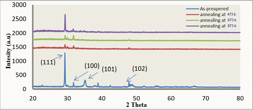
- X-ray diffraction of the thin films before and after the annealing process
- The XRD parameters before and after annealing
Sˣ1014 lines.m-2 | D nm | Strain ˣ10-4 lines-2.m-4 | HKL | 2 Theta | Sample |
As Prepared | 29.28 | 111 | 0.674 | 52.3 | 3.7892 |
31.74 | 100 | 0.670 | 51.6 | 3.7446 |
38.84 | 101 | 0.657 | 52.7 | 3.5983 |
47.82 | 102 | 0.636 | 54.4 | 3.3786 |
200C˚ | 29.34 | 111 | 0.763 | 45.3 | 4.855 |
31.72 | 100 | 0.337 | 1027 | 0.9481 |
47.64 | 102 | 0.452 | 6.5 | 1.7067 |
400C˚ | 29.34 | 111 | 0.754 | 45.8 | 4.7470 |
31.82 | 100 | 7.673 | 95.1 | 4.9010 |
47.82 | 102 | 6.409 | 45.0 | 3.4210 |
600C˚ | 29.36 | 111 | 6.361 | 54.4 | 3.3710 |
31.68 | 100 | 6.917 | 54.7 | 3.3338 |
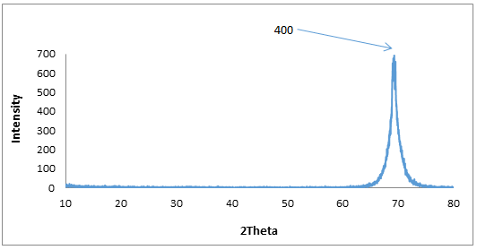
- The X-ray diffraction of the porous silicon
Fig. 3 shows the AFM images of the surface of the prepared membranes before and after the heat treatment. The examination shows that the prepared membranes and annealed membranes are regular and homogeneous in spherical shapes, separated by nano-scale spaces, with a decrease in the RMS value for the prepared membranes before and after the heat treatment as shown in Table 2. It indicates an increase in the granular homogeneity of the prepared membranes as the temperature increases annealing. The best degree of homogeneity of the prepared films was at the highest temperature 600˚C.
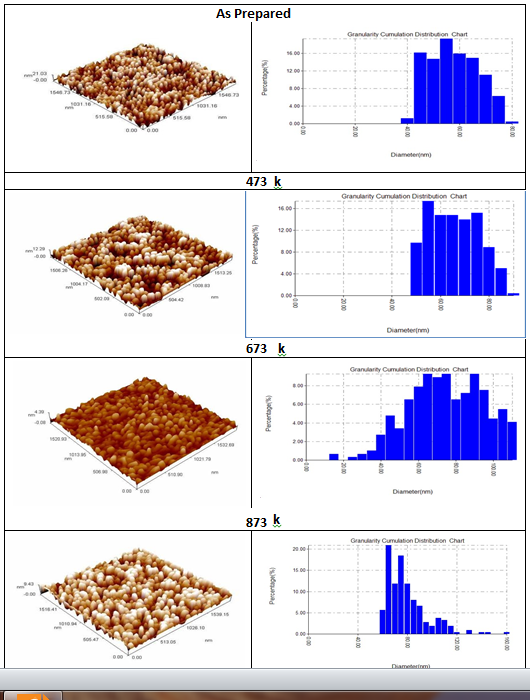
- AFM images for the prepared
 thin films
- The AFM value of parameters
RMS nm | Roughness Average nm | Average Diameter nm | Sample |
6.11 | 5.3 | 55.28 | As Prepared |
3.58 | 3.09 | 63.18 | 200C˚ |
0.506 | 0.40 | 72.15 | 400C˚ |
2.48 | 2.11 | 77.29 | 600C˚ |
Fig. 4 shows the bonds of the prepared films before and after the heat treatment. The examination shows the bonds of the films, which are cd-o bonds within the 830cm-1 within the wave number 850-1000cm-1. The N-O bond at the 1300cm-1 absorption bond within the wave number 1300-2000cm-1, and the O-H bond at the two absorption bonds 3300 within the wave number 3000-3500cm-1 [11]-[18], the bonds become clearer as the annealing temperature increases as a result of the growth of the material at high temperature, especially at a temperature of 600m˚C.
Fig. 5 shows the transmittance spectrum of the prepared films before and after heat treatment within the fixed wavelength range of 300-900nm. It can be noticed that the transmittance decreases after the annealing process, which indicates that the increase in temperature led to a regular arrangement of atoms [19]-[21], and accordingly the transmittance decreases from 55% before annealing to 6% after annealing at 600˚C.
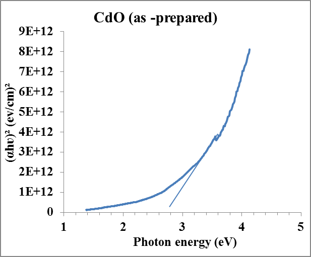
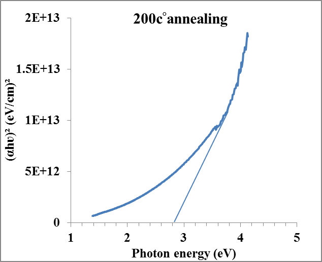
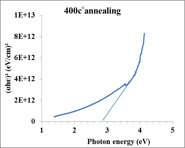
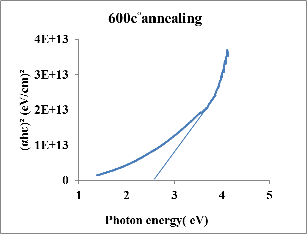
Fig. 6 shows the optical energy gap of the prepared thin films before and after the heat treatment. It can be obtained that the optical energy gap begins to decrease when the heat treatment process is performed, as a result of the generation of local levels as a result of defects that reduce the energy gap as shown in Table 3.
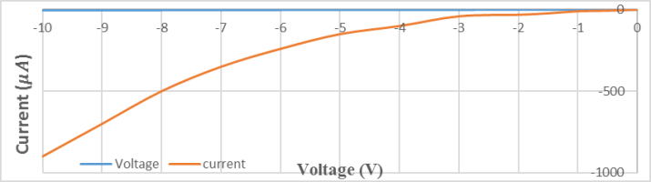
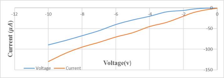
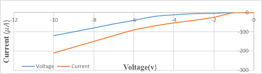
Fig. 7 shows the (I-V) characteristics of the cell in the dark state manufactured from the deposition of the on the porous silicon. All samples are subjected to the annealing process at three different temperatures (200, 400, and 600) ˚C. The process was done in a dark room for all the samples, where the negative parts are connected and the positive part together to each of the samples and the continuous power supply (DC power supply) within a range (0-10) V in case of forward bias. The (I-V) properties of the cell are examined in a dark environment by connecting the negative portion of the sample to the positive portion of the power source while applying reverse bias. The results showed that the dark current increased with the increase of the voltage, where the highest current ratio is at the annealing temperature of (600) ˚C, which means that both the annealing process and porous silicon improved the properties of the material.
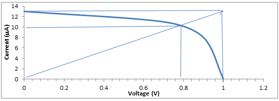
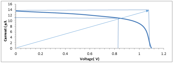
Fig. 8 shows the (I_V) characteristics of the fabricated solar cell when it is exposed to white light. It can be found that an increase in the current with an increase in voltage, and it continues to increase with the increases of the temperature for all the prepared samples in the illumination case.
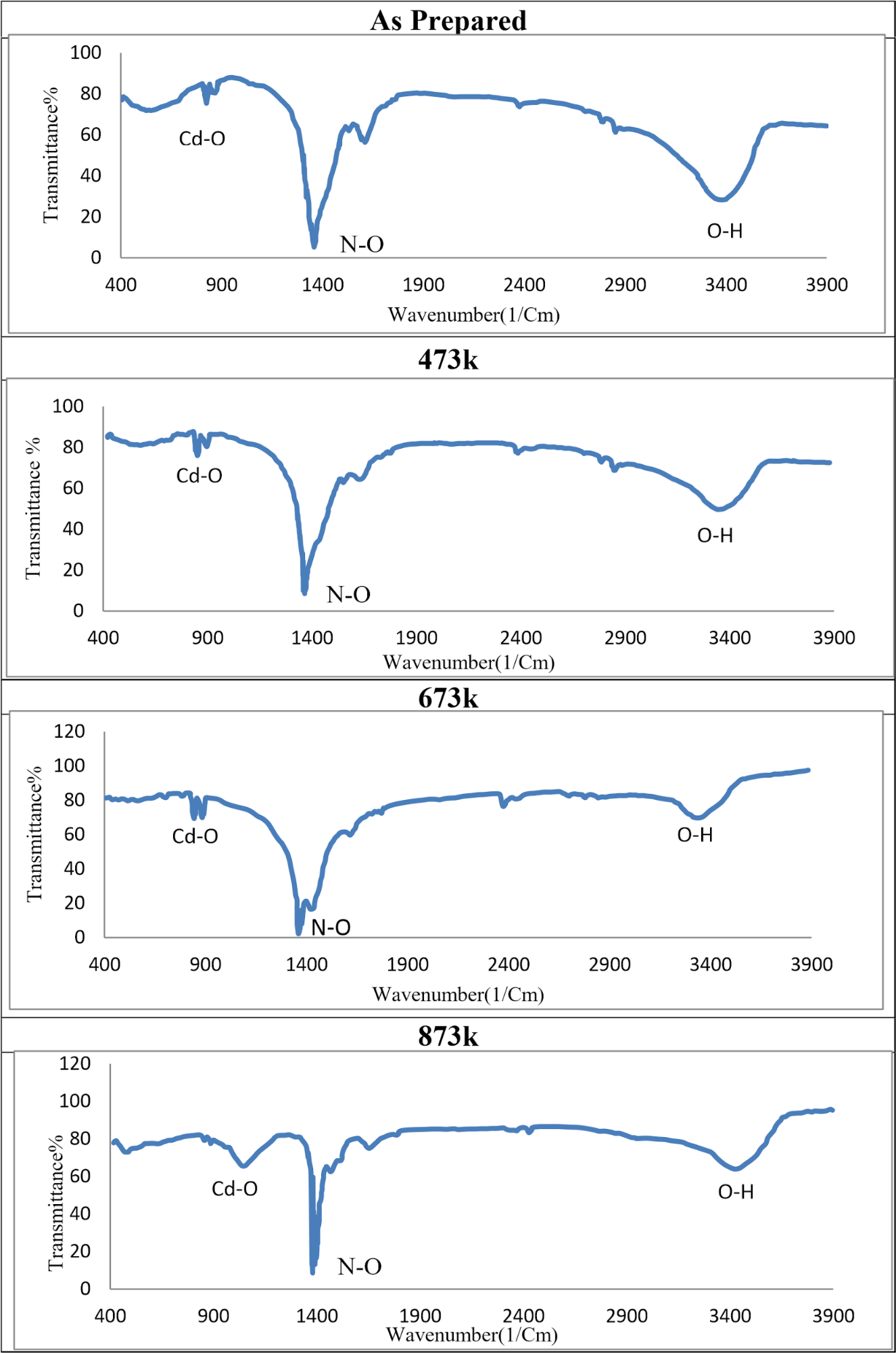
- FTIR of the prepared thin films
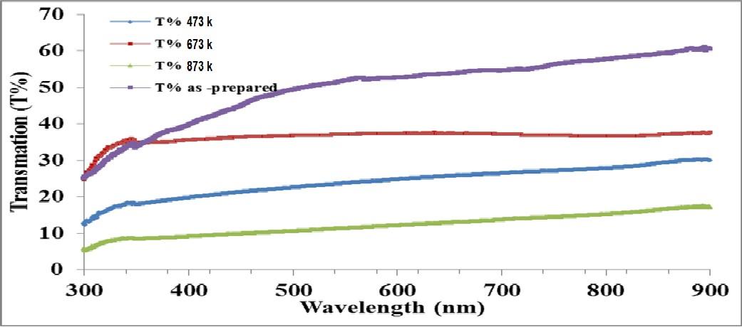
- Transmittance spectrum for the thin films
- Optical energy gap of the thin films
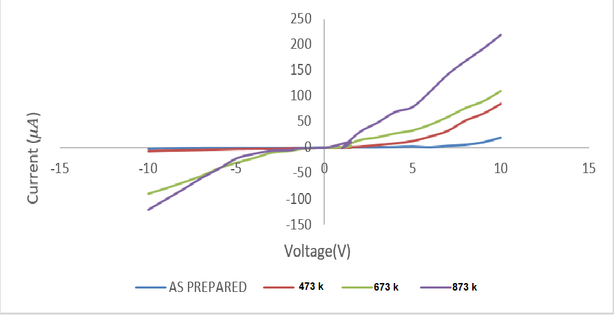
- The current in forward and reverse bias in the dark case for all the samples after the annealing
- The solar cell parameters after the annealing process
- Optical energy gap values of the thin films
Sample | Energy gap (e.V) |
As Prepared | 3 |
200˚C | 2.8 |
400˚C | 2.7 |
600˚C | 2.5 |
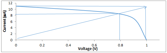
Table 4 shows the contrast between open circuit voltage  and short circuit current , where the current increases with the increase in voltage when the annealing process is performed to reach the highest value of current and voltage, efficiency, filling factor at a temperature of (600) ˚C, can be seen in Fig. 9.
- Solar cell parameters /Psi before and after annealing
- The value of the cell parameters in three different temperatures
Sample | 
( ) ) | 
( ) ) | 
() | 
() | F.F% | η% |
As Prepared | 8 | 1.1 | 6.2 | 0.8 | 62 | 5.8 |
200C˚ | 11 | 1 | 8.5 | 0.8 | 60 | 7.2 |
400C˚ | 13 | 1 | 10 | 0.8 | 61 | 8.5 |
600C˚ | 14 | 1.1 | 11 | 0.8 | 62 | 9.3 |
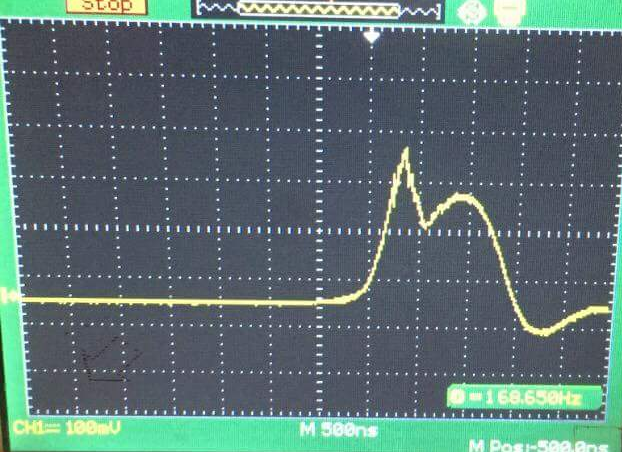
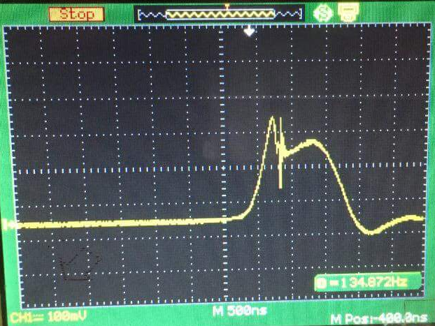
Fig. 10 shows the lifetime carrier for the sample at the annealing in three different temperatures, which is one of the necessities of the cell parameters, considering the average time between the process of the formation of carriers and their union. Therefore, it is important to know the lifetime carrier to determine the efficiency of the cell; the relation between annealing temperature and carrier lifetime is listed in Table 5. It's clear that raising the annealing temperature increases the lifetime carrier. The annealing process leads to an improvement in the characteristics and efficiency of the solar cell.
- The lifetime carrier for the thin films before and after annealing
Sample | /PSi (τ Life) µ sec |
As prepared | 0.004 |
200ᵒC | 0.005 |
400ᵒC | 0.007 |
600ᵒC | 0.019 |
- The lifetime carrier for all the samples in three different temperatures
Conclusions
The preparation of was conducted using the simple chemical method. Analysis of its structural characteristics revealed a multi-cubic crystalline structure, with peaks matching those of cadmium oxide as confirmed by X-ray diffraction (XRD) analysis. Porous silicon was produced by the electrochemical etching technique. followed by the deposition of onto the porous silicon using the drop-casting method. Subsequently, a solar cell was fabricated on the porous silicon, and the properties of this electronic device were studied at three different temperatures (200, 400, and 600) °C during the annealing process.
References
- A. Gulino and G. Tabbì, “CdO thin films: a study of their electronic structure by electron spin resonance spectroscopy,” Applied surface science, vol. 245, no. 1-4, pp. 322-327, 2005, https://doi.org/10.1016/j.apsusc.2004.10.026.
- O. Bisi, S. Ossicini, and L. Pavesi, "Porous silicon: a quantum sponge structure for silicon based optoelectronics," Surface Science Reports, vol. 38, no. 1-3, pp. 1-126, 2000, https://doi.org/10.1016/S0167-5729(99)00012-6.
- F. A. Cotton, G. Wilkinson, C. A. Murillo, and M. Bochmann. Advanced inorganic chemistry. John Wiley & Sons. 1999. https://books.google.co.id/books?hl=id&lr=&id=NFHNEAAAQBAJ.
- T. L. Chu and S. S. Chu, "Degenerate Cadmium Oxide Films for Electronic devices," Journal of Electronic Materials, vol. 9, pp. 1003-1005, 1990, https://doi.org/10.1007/BF02659690.
- H. Eshghi and P. Shalieyoon, “P2O5/SiO2 as a mild and efficient reagent for acylation of alcohols, phenols and amines under solvent-free conditions,” Journal of Chemical Research, vol. 2004, no. 12, pp. 802-805, 2004, https://doi.org/10.3184/0308234043431267.
- R. Ghosh, S. Maiti and A. Chakraborty, " Facile catalyzed acylation of alcohols, phenols, amines and thiols based on ZrOCl2· 8H2O and acetyl chloride in solution and in solvent-free conditions,” Tetrahedron letters, vol. 46, no. 1, pp. 147-151, 2005, https://doi.org/10.1016/j.tetlet.2004.11.006.
- A. A. M. Farag, et al., “Investigating the influence of Eu-doping on the structural and optical characterization of cadmium oxide thin films,” Optik, vol. 281, p. 170830, 2023, https://doi.org/10.1016/j.ijleo.2023.170830.
- R. N. Bulakhe and C. D. Lokhande, “Chemically deposited cubic structured CdO thin films: room temperature,” In AIP Conference Proceedings, vol. 1536, no. 1, pp. 503-504, 2013, https://doi.org/10.1063/1.4810321.
- A. V. Singh, M. Kumar, R. M., Mehra, A. Wakahara, and A. Yoshida, “Al-doped zinc oxide (ZnO: Al) thin films by pulsed laser ablation,” Journal of the Indian Institute of Science, vol. 81, no. 5, p. 527, 2001, https://doi.org/10.1007/BF03179041.
- K. Takahashi, A. Yoshikawa, and A. Sandhu. Wide bandgap semiconductors. Verlag Berlin Heidelberg. 2007. https://doi.org/10.1007/978-3-540-47235-3.
- A. Tadjarodi, M. lmani and H. kerdari, "Application of a facile solid state process to synthesize the CdO sphericall nanoparticles," Internation Nano letters, vol. 3, pp. 1-6, https://doi.org/10.1186/2228-5326-3-43.
- M. J. Alghurabe, D. M. Al-Shamkhee, and A. A. Alsahlani, “Experimental and numerical study of thermal performance for flat plate solar water heater in Najaf,” In IOP Conference Series: Earth and Environmental Science, vol. 877, no. 1, p. 012042, 2021, https://doi.org/10.1088/1755-1315/877/1/012042.
- H. A. Kazem, M. T. Chaichan, A. H. Al-Waeli, R. Al-Badi, M. A. Fayad, and A. Gholami, “Dust impact on photovoltaic/thermal system in harsh weather conditions,” Solar Energy, vol. 245, pp. 308-321, 2022, https://doi.org/10.1016/j.solener.2022.01.026.
- M. K. Abood, M. A. Fayad, H. A. Al Salihi, and H. A. A. Salbi, “Effect of ZnO nanoparticles deposition on porous silicon solar cell,” Materials Today: Proceedings, vol. 42, pp. 2935-2940, 2021, https://doi.org/10.1016/j.matpr.2021.01.833.
- A. Al Ezzi, et al., “Nano-iron oxide-ethylene glycol-water nanofluid based photovoltaic thermal (PV/T) system with spiral flow absorber: An energy and exergy analysis,” Energies, vol. 15, no. 11, p. 3870, 2022, https://doi.org/10.3390/en15113870.
- H. A. Al Salihi, M. A. Fayad, M. Slepchenkov, and V. Shunaev, “Nanoscale oscillator on the base of single-walled carbon nanotube with internal fullerenes C36 and C80,” In Saratov Fall Meeting 2019: Laser Physics, Photonic Technologies, and Molecular Modeling, vol. 11458, pp. 239-245, 2020, https://doi.org/10.1117/12.2564390.
- M. T. Chaichan et al., “Modified Nano-Fe2O3-Paraffin Wax for Efficient Photovoltaic/Thermal System in Severe Weather Conditions,” Sustainability, vol. 14, no. 19, p. 12015, 2022, https://doi.org/10.3390/su141912015.
- M. T. Chaichan et al., “Sand and dust storms’ impact on the efficiency of the photovoltaic modules installed in baghdad: a review study with an empirical investigation,” Energies, vol. 16, no. 9, p. 3938, 2023, https://doi.org/10.3390/en16093938.
- M. T. Chaichan, H, A, Kazem, A. H. Al-Waeli, W. H. Elawee, M. A. Fayad, and K. Sopian, “Advanced techniques for enhancing solar distiller productivity: a review,” Energy Sources, Part A: Recovery, Utilization, and Environmental Effects, vol. 46, no. 1, pp. 736-772, 2024, https://doi.org/10.1080/15567036.2023.2289559.
- H. A. Hussein, Z. Wang, W. K. Alani, J. Zheng, and M. A. Fayad, “A novel experimental design for free energy from the heat-gaining panel using multi-thermoelectric generators (TEGs) panel,” Case Studies in Thermal Engineering, vol. 50, p. 103431, 2023, https://doi.org/10.1016/j.csite.2023.103431.
- S. H. Majeed et al., “Cooling of a PVT System Using an Underground Heat Exchanger: An Experimental Study,” ACS omega, vol. 8, no. 33, pp. 29926-29938, 2023, https://doi.org/10.1021/acsomega.2c07900.
Raghad R. Mahdi, Study of Some Properties of Solar Cell Fabricated by Depositing Cadmium Oxide on Porous Silicon at Varying Temperatures