Journal of Fuzzy Systems and Control, Vol. 2, No 3, 2024 |
|
A Study of In2O3 Nano Particles for Gas Sensor Application
Raghad J. Halbos 1,*, Sariya Al-Algawi 2, Rashed T. Rasheed 3, Ruqia Abdulhussien Hassan 4, Raghad R. Mahdi 5,
Hasanain Azeez 6, M. A. Fayad 7
1,4,5,7 Energy and Renewable Energies Technology Center, University of Technology- Iraq, Baghdad, Iraq
2,3Applied Sciences Department, University of Technology- Iraq, Baghdad, Iraq
6 Civil Engineering Department, University of Technology- Iraq, Baghdad, Iraq
Email: 1 raghad.j.halbos@uotechnology.edu.iq, 4 ruqia.a.hassan@uotechnology.edu.iq,
5 raghad.r.mahdi@uotechnology.edu.iq, 7 mohammed.a.fayad@uotechnology.edu.iq
*Corresponding Author
Abstract— In this research, the sol-gel technique was used to prepare indium oxide nanoparticles. In addition, these particles are deposited by (dip coating technique) on a quartz substrate. Several measurement instruments (FTIR, SEM, UV-visible, and X-RAY diffraction) were used in this study to diagnose and analyze the properties of indium oxide ( ) particles at different parameters. The results from XRD indicated that the particle formation converted to a polycrystalline phase at different annealing temperatures (200 ℃ and 600 ℃) for an hour and a half. Also, the XRD results show an increase in the (grain size and lattice constant) with increased annealing temperature. The measurements of the Hall Effect showed the type of conductivity of () particles is N-type, carrier concentration, mobility, and resistivity. The results of the sensitivity of indium oxide thin films to toxic gas, specifically carbon monoxide (
 ) gas, showed an increase in the sensitivity of thin films annealed at high temperatures.
Keywords—Indium Oxide; Sol-Gel Technique; SEM; X-Ray Diffraction; Sensor
Introduction
Indium oxide is among the important transparent conducting materials, it has a direct band gap energy of up to 3.6 ev at room temperature [1][2]. It was found that there are several factors on which the energy gap of indium oxide depends such as annealing temperature, atmosphere, and the nature of the substrate used to form thin films by depositing the material on them. The increase in the annealing temperature of indium oxide thin films also affects the optical and electrical properties and structural, and morphological of the films. It seems appropriate for different solid-state devices like gas sensors [3], and optoelectronic devices depending on the processing conditions and the electronic properties of the material. Over the past years, due to the wide applications made of nanostructured metal oxide semiconductors (MOSs) in various fields, these materials have attracted great attention from researchers in this field [4][5]. Among various (MOSs), indium oxide () has a wide band gap, good electrical conductivity, excellent optoelectronic properties, and stability [1][6]. Indium oxide is usually doped by tin, cadmium oxide, cadmium, and tin dioxide ( ) specially doped with antimony or fluorine and undoped/doped zinc oxide. They have large energy band gaps in the ultraviolet and are transparent over the visible range [7]. In the present work, nanoparticles are prepared by the Sol-Gel method and used as gas sensor applications will be studied.
Experimental setup
There are many ways to prepare indium oxide nanoparticles; the method used in this work is the sol-gel method. This method is easy, fast, and rapid to prepare nanoparticles in accepted amounts. The method is as follows: dissolving indium nitrate ( ) with distilled water, to ensure complete dissolution for the solution (0.3 M), we used a magnetic capsule (magnetic stirrer). The dissolving process is carried out at a temperature of (30 ℃) for (25 minutes). As in the previous step, salt hydroxide (
 ) was dissolved in distilled water at (30 ℃) for 25 minutes using the same method.
Then the dissolved sodium hydroxide solution is added to the dissolved indium nitrate solution in the form of drops at a rate of (3 drops per minute), while the stirring process continues until the pH value is reached [8]. To clean the chemical compound resulting from the reaction from unwanted impurities, the compound is washed with pure water several times and then washed twice with ethyl alcohol, the final step is to dry the resulting material at (200 ℃) for an hour and a half, we get a white powder, when the annealing temperature increases to (600 ℃), the precipitate turns yellow as shown in Fig. 1.
The general chemical equations for the reaction are:


------------------------------------------------------------------------
The overall equation is:
Among the methods used to form indium oxide thin films is the dip coating method. As the substrate (quartz) is immersed in the solution, it is pulled out continuously. During the 25-second immersion period, the substrate remains submerged in the solution; then it is dried at 100 ℃ for 6 minutes. By dipping the substrate, we can control the thickness of the films, and the number of immersions about (15- 30 dip).
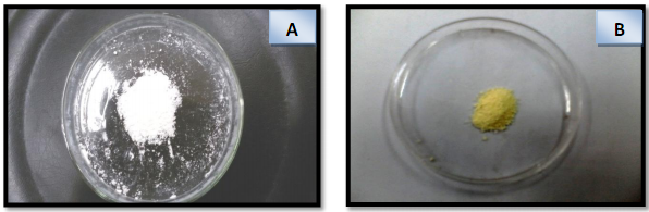
- A- indium hydroxide after drying at 200 ℃ B-indium oxide after annealing at 600 ℃
Results and discussion
XRD Results for In2O3 Particles
The XRD is used for the identification and understanding of the crystalline growth nature of particles that are prepared by the sol-gel method. An important factor that effects on structure of indium oxide particles is the annealing temperature. The X-ray diffraction device (XRD) is used to analyze and extract information about the physical properties, structure, and crystalline of the indium hydroxide at (200 ℃) as prepared and for indium oxide particles annealed at an annealing temperature of 600 ℃.
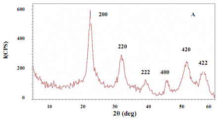
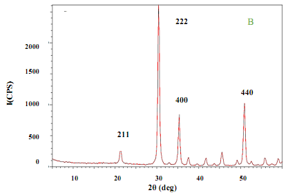
The XRD results (Fig. 2) for indium hydroxide at 200 ℃ indicate the formation of diffraction patterns at the 2θ values are 22.4494°, 31.944°, 51.4602° and 56.5230° corresponding to (200), (220), (420) and (422), respectively. All measurements we obtained from XRD indicate formation (body-center cubic indium hydroxide) according to the (JCPDS Card No. 01-076-1463). Based on the XRD spectra of the particles, it can be found that they are polycrystalline and cubic, and this agrees with the previous study [8].
Through the results of XRD, we notice that the intensity of plane (222) increases as a function of annealing temperature which may be due to the increasing grain size of particles. When the annealing temperature increases, the interplanar distance (d) increases as a result of oxidation processes, and this leads to an increase in the lattice constant [9]. All XRD results are shown in Table 1. (A: indium hydroxide and B: indium oxide).
- The measurements of the XDR for as prepared and at annealing temperatures (200 and 600 ℃) for 90 min
Annealing Temperature for 90min | 2θ (deg) | hkl | FWHM (β) (deg) | Grain Size(A°) | Lattice constant (A°) | d (A°) |
200 ℃ As-prepared | 22.4494 | 200 | 1.5794 | 51.280326 | 7.914459 | 3.95722 |
31.944 | 220 | 1.9994 | 41.328914 | 7.917615 | 2.79929 |
51.4602 | 420 | 2.6985 | 32.679875 | 7.935119 | 1.77434 |
56.5230 | 422 | 2.42340 | 37.218146 | 7.969824 | 1.62683 |
600 ℃ | 21.3455 | 211 | 0.63550 | 127.2090 | 10.18817 | 4.15930 |
30.4441 | 222 | 0.5968 | 137.9548 | 10.16297 | 2.93379 |
35.3310 | 400 | 0.5913 | 141.0019 | 10.15358 | 2.53839 |
50.8974 | 440 | 0.6081 | 144.6793 | 10.14067 | 1.79263 |
|
(A) |
|
(B) |
- XRD patterns of indium oxide particles: (A) as-prepared
 powder (B) at annealing temperature 600 ℃
Fourier Transform Infrared Spectroscopy (FTIR)
FTIR is a technique used to obtain an infrared spectrum of the absorption or emission of a substance as shown in Fig. 3. Infrared spectra can help determine the chemical structure or bonds present in an unknown molecule. After obtaining the FTIR spectrum, the scan can be interpreted to provide information about the compound present in the test sample. It is compared to the spectra of standard materials, as the spectrum gives important information about the sample. For instance, Peng et al. found that in the reaction system, to obtain In2O3 nanocrystals, hydrolysis, and alcoholysis were the major reaction pathways for the indium precursors [10].
Table 2. shows some of the important peaks of indium nitrate and prepared indium oxide.
- Absorption bands (cm–1) in the FTIR spectra of the , , and annealing at 400 and 600 ℃
| Indium oxide |
Asprepared () | Annealing at 600 ℃ |
3650  stretching stretching | 3500 stretching. | 3419 stretching |
1620  bending bending | 1635 bending | 1622 bending |
1384  asymmetric and symmetric asymmetric and symmetric | 1367  stretching stretching | 606 bending |
825  bending. bending. | 1167 due to surface reaction of the nanoparticles with the atmosphere | 567,540,491,457 In-O stretching
|
- | 775 stretching | - |
- | 503  stretching stretching | - |
FTIR spectrum of () as prepared. Spectral analysis shows a strong absorption band around 3500 cm-1 in this spectrum, even after annealing at high temperatures, it is difficult to completely remove water residues from  stretching [11]. Furthermore, the results in Fig. 4 indicated that In-O(H) and In-O exhibit stretching peaks at 775 and 503 cm-1, respectively. A prominent absorption band can be seen for (600 ℃). The peaks at (3420 cm-1) indicate the main peaks of water absorption, while the low wave peaks (601, 567, 540, 491, and 457 cm-1) indicate the bond. These results are consistent with the results of thermal analysis [12].
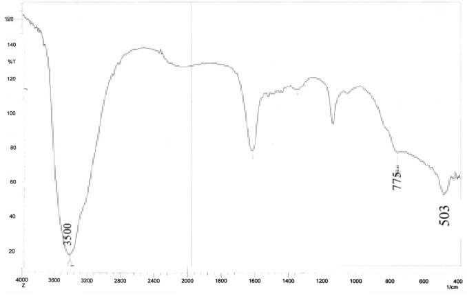
- FTIR transmittance spectrum of as-prepared (200 ℃) as a function of wavenumber
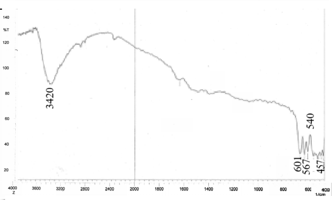
- FTIR transmittance spectrum of at (600 ℃) as a function of wavenumber
Surface Morphology by (SEM)
The structure of particles (as-prepared and annealed at 600 ℃) is prepared by sol-gel technology and was examined by using a scanning electron microscope (SEM). Fig. 5 (A) shows an image of the as-prepared indium hydroxide particles measured by SEM technique. It is clear, at low annealing temperatures the results show that particles of small sizes are formed. While at high annealing temperatures, the size of indium oxide particles is large, as shown in Fig. 5. (B), this was due to the growth and combination of small grains together after the sintering process.
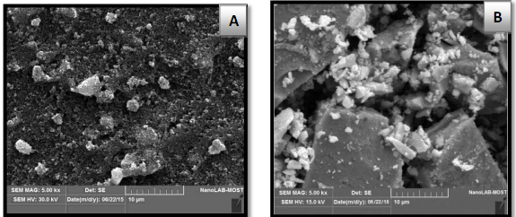
- SEM image of In2O3 particles (A) as-prepared (B) annealing at 600 ℃
Optical Properties
The transmission of indium oxide films is affected by several factors, the most important of which is the annealing temperature of thin films, and this is shown in Fig. 6. The transmission of the films is high, reaching (74.8 %) in the visible region at 600 ℃. At (200 ℃) the transmittance values are (64.5 %) respectively. The transmission of films increases when the annealing temperature increases; there was an improvement in the particle's structural homogeneity and crystallinity, which can be attributed to this. These results are compatible with prior work [13].
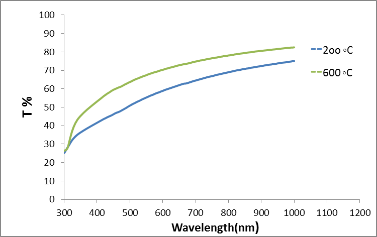
- The results of (UV-visible) transmittance spectra of indium oxide thin films at (200 and 600 ℃)
In this study, a UV/visible spectrometer was used to obtain the transmittance and reflectance spectrum of indium oxide thin films in order to measure the energy gap of this material through its transmittance spectrum. However, the reflectance spectrum is very small and is neglected in the calculations when measuring the energy gap. The energy gap represents the thin films.
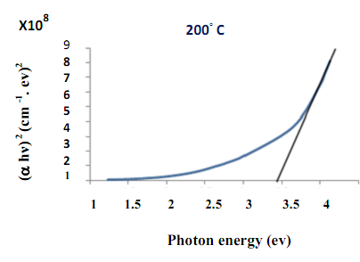
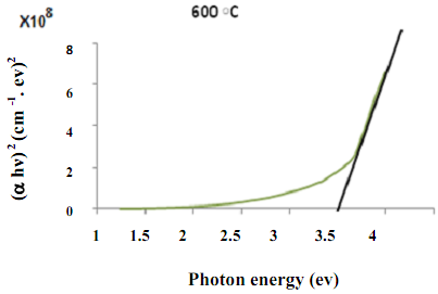
The results indicate an increase in the energy gap of indium oxide thin films annealed at high temperatures compared to lower annealing temperatures, as the band gap and the annealing temperature of indium oxide are directly proportional as shown in Fig. 7 and Table 3. This may be due to the removal of the surface defect an increase in grain size and a decrease in grain boundaries by heat treatments, this change is also due to the increase in the concentration of the number of carriers, as this increase fills the lower energy of the conduction band which is known as Broston-Moss effect (10,14). By plotting (αhν)2 versus photon energy (hν) and projecting a straight line, we can measure the energy band gap.
- The results of energy band gap measurements for indium oxide at the different annealing temperatures
Different condition | Eg (eV) |
Effect of annealing temperature | As prepared | 3.4 |
600 ℃ | 3.5 |
- A plot of (α hν) 2 verses (hν) of indium oxide thin films at (as prepared and 600 ℃)
The Results of The Hall Effect of Indium Oxide
Hall measurements are used to obtain information about the conductivity of the substance, the amount of carrier concentration, as well as the mobility and resistivity of the indium oxide. Hall measurements are taken for indium oxide thin films as a prepared material at a temperature of 200 ℃ and also as an annealed material at a temperature of 600 ℃ for an hour and a half, halls results show that the conductivity of indium oxide is n-type, also the results indicate an increase in the concentration of carriers directly with an increase in annealing temperature and this results agree with Halbos et al. [15]. As shown in Table 4, the Hall coefficient and Hall mobility decrease as the annealing temperature increases. The scattering occurring in semiconductors can be the reason for the decrease in hall mobility 14.
- Hall measurements for indium oxide at different annealing temperatures (200 ℃ and 600 °C)
Sample Thin | Carrier concentration (cm)-3 | μH (cm2/v∙s) | RH (cm3/ C) |
/200 ℃ | 5.5˟1011 | 7.3˟10 | 1.1˟107 |
/600 ℃ | 1.9˟1015 | 2.4˟102 | 3.2˟103 |
Gas sensor measurements
To measure the sensitivity properties of indium oxide films to toxic gases, specifically gas, as a function of operating time at a specific temperature (50 ℃). gas had a concentration ratio of 5 parts per million. To measure the sensitivity of an indium oxide thin film to CO gas [16]-[20], it is measured in two states: air and in CO gas at a temperature of (50 ℃). When gas is present, the surface resistance of the indium oxide thin films changes at a certain rate of time, and the sensitivity can be measured by using this equation (1).

| (1) |
The symbol (Ra) indicates the electric resistance of the gas sensor (indium oxide thin film) in the presence of air, while the symbol (Rg) air indicates the electric resistance of the gas sensor (indium oxide thin film) in the presence of gas (). The sensitivity (S) increases from 200 to 600 ℃ is presented in Fig. 8, the highest percentage of sensitivity to CO gas we obtained was for the () thin films annealed at a temperature (600 ℃), where it reached (70%). The results agree with the results in previous studies [20]-[25]. Due to their high resistance, indium oxide thin films do not work as prepared.
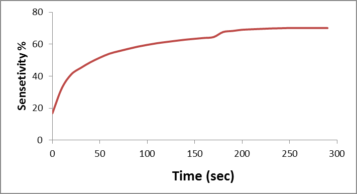
- Sensitivity of indium oxide thin films at (600 ℃) for gas
Conclusions
Through the results, we obtained that the X-ray diffraction measurement shows that indium oxide particles have a polycrystalline structure and also have excellent crystalline, as this property increases with increasing annealing temperature. The results of the SEM for indium oxide particles show an increase in particle size when the annealing temperature is increased. This was due to the growth and combination of small grains together after the sintering process. Transmittance spectrum measurements for films annealed at 600 ℃ reached approximately (78%). The results of the energy gap of indium oxide films indicate an increase in the gab proportional to the increase in the annealing temperature. The results of Hall measurements showed that indium oxide thin films have a negative Hall coefficient (RH) value which confirms that films are (n-type). The sensitivity increases from 200 to 600 ℃.
References
- E. A. Forsh, et al., “Optical and photoelectrical properties of nanocrystalline indium oxide with small grains,” Thin Solid Films, vol. 595, pp. 25-31, 2015, https://doi.org/10.1016/j.tsf.2015.10.053.
- P. Li and H. Fan, “Porous In2O3 microstructures: hydrothermal synthesis and enhanced Cl2 sensing performance,” Materials Science in Semiconductor Processing, vol. 29, pp. 83-89, 2015, https://doi.org/10.1016/j.mssp.2013.09.026.
- M. Seetha, D. Mangalaraj, and Y. Masuda, “Medium dependent size and shape tuning of indium oxide nanoparticles and their gas sensing properties,” Advanced Science, Engineering and Medicine, vol. 3, no. 3, pp. 202-212, 2011, https://doi.org/10.1166/asem.2011.1106.
- S. Bera, M. Pal, S. Sarkar, and S. Jana, “Hierarchically structured macro with nested mesoporous zinc indium oxide conducting fil,” ACS Applied Materials & Interfaces, vol. 9, no. 5, pp. 4420-4424, 2017, https://doi.org/10.1021/acsami.6b13143.
- H. Khan, S. Sarkar, M. Pal, S. Bera, and S. Jana. Indium Oxide Based Nanomaterials: Fabrication Strategies, Properties, Applications, Challenges and Future Prospect. In Post-Transition Metals. IntechOpen. 2020. https://doi.org/10.5772/intechopen.94743.
- O. Bierwagen, “Indium oxide—a transparent, wide-band gap semiconductor for (opto) electronic applications,” Semiconductor Science and Technology, vol. 30, no. 2, p. 024001, 2015, https://doi.org/10.1088/0268-1242/30/2/024001.
- R. R. Mahdi, S. A. Maki, H. H. A. Salihi, M. K. Abood, R. J. Halbos, R. A. Hassan, and M. A. Fayad, “Study Some Properties of Solar Cell Fabricated by Deposited Cadmium Oxide on Pours Silicon in Three Different Temperatures,” Journal of Fuzzy Systems and Control, vol. 2, no. 2, pp. 87-91, 2024, https://doi.org/10.59247/jfsc.v2i2.179.
- C. Aparna, M. G. Mahesha, and P. K. Shetty, “Structural and optical properties of indium oxide thin films synthesized at different deposition parameters by spray pyrolysis,” Materials Today: Proceedings, vol. 55, pp. 141-147, 2020, https://doi.org/10.1016/j.matpr.2022.01.048.
- A. Ayeshamariam, M. Bououdina, and C. Sanjeeviraja, “Optical, electrical and sensing properties of In2O3 nanoparticles,” Materials Science in Semiconductor Processing, vol. 16, no. 3, pp. 686-695, 2013, https://doi.org/10.1016/j.mssp.2012.12.009.
- W. Shirbeeny and W. E. Mahmoud, “Synthesis and characterization of transparent optical gas sensor device made of indium oxide pyramid like nanoarchitectures,” Sensors and Actuators B: Chemical, vol. 191, pp. 102-107, 2014, https://doi.org/10.1016/j.snb.2013.09.058.
- G. Liu, “Synthesis, characterization of In2O3 nanocrystals and their photoluminescence property,” International Journal of Electrochemical Science, vol. 6, no. 6, pp. 2162-2170, 2011, https://doi.org/10.1016/S1452-3981(23)18174-0.
- R. J. Halbos, S. Al-Algawi, and R. T. Rasheed, “Synthesis and characterization of IZO composite prepared by sol-gel method,” Al-Nahrain Journal of Science, vol. 19, no. 3, pp. 39-47, 2016, https://doi.org/10.22401/JNUS.19.3.06.
- M. Kraini, N. Bouguila, I. Halidou, A. Timoumi, and S. Alaya, “Properties of In2O3 films obtained by thermal oxidation of sprayed In2S3,” Materials Science in Semiconductor Processing, vol. 16, no. 6, pp. 1388-1396, 2013, https://doi.org/10.1016/j.mssp.2013.04.021.
- M. Shakiba, A. Kosarian, and E. Farshidi, “Effects of processing parameters on crystalline structure and optoelectronic behavior of DC sputtered ITO thin film,” Journal of Materials Science: Materials in Electronics, vol. 28, pp. 787-797, 2017, https://doi.org/10.1007/s10854-016-5591-1.
- R. J. Halbos, S. AL-Algawi, and R. T. Rasheed, “Gas Sensitivity of ITO Composite Prepared by Sol-Gel Method,” Engineering and Technology Journal, vol. 35, no. 10 (Part A), 2017, https://doi.org/10.30684/etj.35.10A.3.
- G. E. Patil et al., “Synthesis, characterization and gas sensing performance of SnO 2 thin films prepared by spray pyrolysis,” Bulletin of Materials Science, vol. 34, pp. 1-9, 2011, https://doi.org/10.1007/s12034-011-0045-0.
- M. J. Alghurabe, D. M. Al-Shamkhee, and A. A. Alsahlani, “Experimental and numerical study of thermal performance for flat plate solar water heater in Najaf,” In IOP Conference Series: Earth and Environmental Science, vol. 877, no. 1, p. 012042, 2021, https://doi.org/10.1088/1755-1315/877/1/012042.
- H. A. Kazem, M. T. Chaichan, A. H. Al-Waeli, R. Al-Badi, M. A. Fayad, and A. Gholami, “Dust impact on photovoltaic/thermal system in harsh weather conditions,” Solar Energy, vol. 245, pp. 308-321, 2022, https://doi.org/10.1016/j.solener.2022.09.012.
- M. K. Abood, M. A. Fayad, H. A. Al Salihi, and H. A. A. Salbi, “Effect of ZnO nanoparticles deposition on porous silicon solar cell,” Materials Today: Proceedings, vol. 42, pp. 2935-2940, 2021, https://doi.org/10.1016/j.matpr.2020.12.771.
- A. Al Ezzi et al., “Nano-iron oxide-ethylene glycol-water nanofluid based photovoltaic thermal (PV/T) system with spiral flow absorber: An energy and exergy analysis,” Energies, vol. 15, no. 11, p. 3870, 2022, https://doi.org/10.3390/en15113870.
- M. T. Chaichan et al., “Modified nano-Fe2O3-paraffin wax for efficient photovoltaic/thermal system in severe weather conditions,” Sustainability, vol. 14, no. 19, p. 12015, 2022, https://doi.org/10.3390/su141912015.
- H. A. Al Salihi, M. A. Fayad, M. Slepchenkov, and V. Shunaev, “Nanoscale oscillator on the base of single-walled carbon nanotube with internal fullerenes C36 and C80,” In Saratov Fall Meeting 2019: Laser Physics, Photonic Technologies, and Molecular Modeling, vol. 11458, pp. 239-245, 2020, https://doi.org/10.1117/12.2564390.
- H. A. Hussein, Z. Wang, W. K. Alani, J. Zheng, and M. A. Fayad, “A novel experimental design for free energy from the heat-gaining panel using multi-thermoelectric generators (TEGs) panel,” Case Studies in Thermal Engineering, vol. 50, p. 103431, 2023, https://doi.org/10.1016/j.csite.2023.103431.
- P. Nemec, A. Čaja, and M. Malcho, “Mathematical model for heat transfer limitations of heat pipe,” Mathematical and Computer Modelling, vol. 57, no. 1-2, pp. 126-136, 2013, https://doi.org/10.1016/j.mcm.2011.06.047.
- R. R. Mahdi, S. A. Maki, H. A. A. Salihi, M. K. Abood, R. J. Halbos, R. A. Hassan, and M. A. Fayad, “Enhancement of the properties of solar cells fabricated by cadmium oxide deposited on porous silicon,” Journal of Fuzzy Systems and Control, vol. 2, no. 1, pp.36-39, 2024, https://doi.org/10.59247/jfsc.v2i1.175.
Raghad J. Halbos, A Study of In2O3 Nano Particles for Gas Sensor Application