Journal of Fuzzy Systems and Control, Vol. 3, No 3, 2025 |
Study, Design, Modeling, Simulation, and Control Analysis of DC-DC Power Converters
Salam Waley Shneen 1,*
1 Energy and Renewable Energies Technology Center, University of Technology, Baghdad, Iraq
Email: 1 salam.w.shneen@uotechnology.edu.iq
*Corresponding Author
Abstract—Researchers are interested in studying power electronics converters because of their importance in many fields and applications, including industrial, agricultural, and domestic applications. Power electronics converters are relatively economical compared to conventional converters. In this work, the researchers present research contributions, including a study on how to design a DC-DC converter from a constant electrical quantity at the converter's input to a variable quantity depending on the load requirements associated with the converter's output. As another research contribution, the researchers are working on building a model of a DC-DC converter. The third contribution is conducting tests using the model and simulating the converter using the engineering computer program MATLAB. Performance is evaluated, ways to improve the converter's operation are identified, and its behavior is analyzed during the transient and steady-state operation periods. Power electronics converters are used to increase the voltage, called a boost converter. There is a type used to decrease the voltage, called a buck converter. Another type combines both states, depending on the system requirements, called a buck-boost converter. Tests are conducted to identify how the converter can be used to meet the load requirements associated with the converter output. They also identify how to control system state changes during operation and how to counter fluctuations resulting from various factors. To adequately cover the load, efforts are made to regulate and improve the performance of the converter by regulating the electrical power to suit this. The converter design is developed to provide the required voltage and current for efficient operation.
Keywords—Open Loop System; Closed Loop System; Pulse Width Modulation (PWM); Boost DC-DC Converter; Buck DC-DC Converter; Buck-Boost DC-DC Converter
Sustainable development is a major concern for researchers and government institutions worldwide. Systems that operate on clean and environmentally friendly energy are capable of meeting the electrical energy requirements for operating various systems in all fields and applications from a variety of sources [1], [2]. Renewable energies, such as wind and solar, are among the most important environmentally friendly sources, and have been incorporated into many fields, requiring further research and development [3], [4]. Electronic power converters are linked to electrical power systems through generation, transmission, and distribution [5], [6]. Electronic power converters are of various types, some classified according to the type of input and output power, others according to the number of phases, and also according to function. The first type can be classified as a step-up or step-down converter [7], [8]. There are also single-phase and three-phase converters [9], [10]. Other classifications are based on input and output current, including AC to AC converters, DC to DC converters, AC to DC converters, and DC to AC converters [11], [12]. Converters operate according to the function, depending on the load requirements and available power source. The first use is when a constant voltage and frequency AC source is available while the AC load requires a change in voltage or frequency, as in controlling the speed of single-phase or three-phase induction motors [13], [14]. The second use is when a DC source, such as solar power, a DC generator, or other sources, is available to cover the DC load requirements. The available voltage may not be sufficient to cover the load requirements, so a converter can be added to regulate the appropriate voltage [15], [16]. The third use is when an AC voltage is available while the load requires DC, a rectifier-type converter is added to convert the AC to DC to cover the load requirements [17], [18]. The fourth use is when a DC voltage is available while the load requires AC, an inverter-type converter is added to convert the DC to AC to cover the load requirements [19], [20].
Converters perform the conversion function using electronic power devices, such as semiconductors, such as diodes, thyristors, and transistors [21], [22]. They operate by switching on and off, regulating the operating periods of these switches, and changing their operating angle. Modern technologies such as pulse width modulation (PWM) can be used with these switches, which help regulate and improve performance and quality [23], [24]. Other methods that help improve the performance of electronic power converters include the use of conventional, expert, and intelligent control units [25], [26]. The ability to regulate and control the converter output makes it a successful choice for many fields and applications using pulse width modulation (PWM) technology [27], [28].
Power electronics converters are used in systems that generate electrical energy from renewable and clean energy sources, such as solar power systems. They are also used in storage systems, such as battery charging and communication systems [29]. The input of the converter is connected to a DC source, such as a solar power source, while the output is connected to a DC load [30]. The converter is built using electronic switches, which are semiconductor devices such as diodes and transistors, such as MOSFETs, IGBTs, and thyristors. Passive components are used to eliminate ripples in the current wave and regulate the output voltage. An inductor or inductor is used to limit ripple, while a capacitor or capacitor acts as a filter to regulate the voltage [17]. Simulation is used to identify system behavior and operation under different conditions, using a system model. After constructing a converter simulation model, it can be run, obtaining the proposed test results, and analyzing those results to verify its effectiveness [31], [32]. Electrical quantities such as current, voltage, power, and efficiency of a transformer can be obtained by placing sensors to measure these quantities for all components of the system (switches, converter, rectifier, filter) [33]. These quantities can be controlled by changing system parameters such as the inductance of the coil, the capacitance of the capacitor, and the gate firing angle of electronic switches (MOSFETs, thyristors, or IGBTs) [34].
The main problem when working with and operating a DC-DC converter is the irregularity of voltage levels in the power source, which causes malfunctions. Several control methods are used to address this malfunction in the converter's operation, including both analog and digital control methods. When the converter's input is irregular, one of these methods is used to control the output and achieve a stable and specific voltage under different load conditions. To obtain the required and appropriate values, tests are conducted to arrive at a suitable design for a high-efficiency and highly reliable system model. This work aims to provide a methodology and overview of design methods for control techniques that enable high-level performance improvement for DC-DC converters. The basic concepts of how these techniques work with a DC-DC converter will also be discussed.
The operation of a power electronic converter can be described by operating a linear system for a specified period of time to identify the system's transition and steady-state conditions at a constant load. To identify nonlinear system behavior, the system's parameters are changed, resulting in fluctuations in instrument readings. To address fluctuations and disturbances, a closed-loop system is adopted, applying feedback to overcome the change resulting from the transient state. A controller can also be used to regulate the converter's output as the load changes and return the system to a steady state.
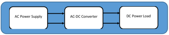
There are many types of the power electronics converters include, first single phase AC-AC converter that show in
Fig. 1. Second, three phase ac-ac converter that show in
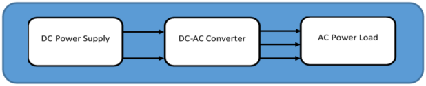
Fig. 2. Third, AC-DC power electronic converter with single phase input power that show in Fig. 3. Fourth, AC-DC power electronic converter with three phase input power that show in Fig. 4. Fifth, DC-DC power electronic converter that show in Fig. 5. Sixth, DC-AC power electronic converter with three phase output power that show in Fig. 6. Sixth, DC-AC power electronic converter with single phase output power that show in Fig. 7.
The mathematical relationships representing the DC-DC converter model can be written by using laws such as Ohm's law, Kirchhoff's current law, and Kirchhoff's voltage law, and applying them to the loops and components of the system depicted in Fig. 8 and the equations below:
First, the differential equations of the DC-DC buck converter are given in vL: Inductor voltage in (1) and ic: Capacitor current in (2). Where IL is the inductor current, Vo is the load and capacitor voltage, Vin is the DC input voltage, u is the discontinuous control, U is the energy stored in the capacitor as in (3), and W is the energy stored in an inductor as in (4).
| (1) |
| (2) |
| (3) |
| (4) |
Fig. 9 shown design of a closed-loop system for a DC-DC Converter that by uses a PI Controller that includes two steps: first, calculate the proportional gain (kp), second, calculate the integral gain (ki). Where the integration time (Ti), critical gain (Kcr), and the period of oscillation (Pcr).
|
This system is designed as a step-down voltage converter. The design process begins with calculations during the operating cycle, which are determined using mathematical relationships represented in steps. First, the inductor voltage is calculated, which involves the ratio of the output voltage to the input voltage of the system, as shown in (1). Second, the capacitor current is calculated, which is the difference between the inductor current and the output current, as shown in (2). Third, the inductor and capacitor power are calculated, as shown in (3) and (4). The (3) shows how to calculate the capacitor power by multiplying the square of the voltage by half the capacitance, while (4) shows how to calculate the inductor power by multiplying the square of the current by half the inductance. Other calculations include the duty cycle of the DC-DC converter, which is calculated using (5), equal to one minus the ratio of the output voltage to the input voltage. The (6) calculates the minimum inductance. This minimum value is calculated from the relationship between the operating cycle (calculated from (5)), minus one, multiplied by the resistance representing the system load, and divided by twice the frequency, as shown in (6). It also involves calculating the value of the inductor by multiplying the minimum inductance by 1.25, as shown in (7). Furthermore, it involves calculating the value of the capacitor from the mathematical relationship representing the ratio of the operating cycle difference minus one, divided by eight times the inductance multiplied by the square of the frequency, and divided by the ratio of the change in output voltage to the output voltage, as shown in (8). The parameter values shown in Table I and Table II are used to implement the design steps. Similarly, the mathematical relationships for step-up transformers and step-down/step-down transformers can be written in steps as shown in Table III to Table VI.
Parameters | Voltage source | Output Voltage | Load | Frequency | ripple |
Symbols | Vs | Vo | R | f | r |
Value | 48 | 18 | 10 | 40000 | 0.5 |
Unit | volt | volt | ohm | Hz | % |
Parameters | Voltage source | Output Voltage | Load | Frequency | ripple |
Symbols | D | Lmin | L | C | D |
Value | 0.375 | 78 | 97.5 | 100 | 0.375 |
Unit | - | μH | μH | μF | - |
Parameters | Voltage source | Output Voltage | Load | Frequency | ripple |
Vs | Vo | R | f | r | Vs |
12 | 24 | 10 | 40000 | 0.5 | 12 |
volt | volt | ohm | Hz | % | volt |
Parameters | Voltage source | Output Voltage | Load | Frequency | ripple |
Symbols | D | Lmin | L | C | D |
Value | 0.375 | 78 | 97.5 | 100 | 0.375 |
Unit | - | μH | μH | μF | - |
Parameters | Voltage source | Output Voltage | Load | Frequency | ripple |
Symbols | Vs | Vo | R | f | r |
Value | 18 | 12 | 10 | 40000 | 1 |
Unit | volt | volt | ohm | Hz | % |
Parameters | Voltage source | Output Voltage | Load | Frequency | ripple |
Symbols | D | Lmin | L | C | D |
Value | 0.4 | 45 | 45 | 100 | 0.4 |
Unit | - | μH | μH | μF | - |
This work presents a suitable virtual environment for a power source similar to the operating environment in any application that requires converting a 12 V source voltage to power a load at a specified voltage of 24 V. The load capacity and power source limitations were taken into account, and the load value and switching frequency of the electronic switches for the boost converter were determined. The default model can be applied to a solar system and a storage battery, with the converter connected to the battery on the output side and to the solar source on the input side [35], [36]. The first research contribution is the study, design, and simulation of a boost converter model that equips the circuit with a 12 V DC source connected to a converter that outputs a 10 Ω load, requiring a 24 V DC supply. The system consists of a switch operated at a frequency of 40,000 Hz for both on and off periods. The system parameters are used to calculate the system components in the model design steps, including calculating the duty cycle using the equation in (5). The resulting value is 0.5, which can be represented as a percentage of 50%. The second design step is to calculate the inductance value in Henrys from the equation in (6), yielding 15.625 μH. The third step is to calculate the inductance value from the equation in (7), yielding 19.53 μH. The fourth step is to calculate the minimum value of the capacitance from the equation in (8), yielding 25 microfarads at r equal 0.05. Mathematical representation of a boost converter. This type can be expressed mathematically as in the mathematical relationships in (5) to (8).
| (5) |
| (6) |
| (7) |
| (8) |
This work presents a suitable virtual environment for a power source similar to the operating environment in any application that requires converting a 48 V source voltage to power a load at a specified voltage of 18 V. The load and power source capabilities were taken into account, and the load value and switching frequency of the electronic switches for the buck converter were determined. The second research contribution is the study, design, and simulation of a model of a converter-pocket that equips the circuit with a 48 V DC source connected to a converter that outputs a 10 Ω load, requiring an 18 V DC supply. The system consists of a switch operated at a frequency of 40,000 Hz for both on and off periods. System parameters are used to calculate the system components in the model design steps, including calculating the duty cycle using the equation in (9). The resulting value was 0.375, which can be represented as a percentage of 37.5%. The second design step was to calculate the inductance value in Henrys from the equation in (10), yielding 78 μH. The third step was to calculate the inductance value from the equation in (11), yielding 97.5 μH. The fourth step was to calculate the minimum value of the capacitance from the equation in (12), yielding 100 μF.
| (9) |
| (10) |
| (11) |
| (12) |
|
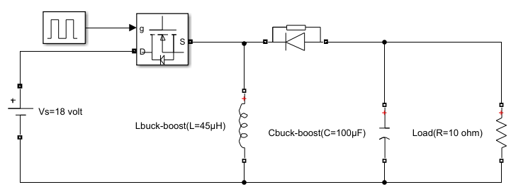
This work presents a suitable virtual environment for a power source similar to the operating environment in any application that requires converting an 18 V source voltage to power a load at a specific voltage higher or lower than 18 V, such as 12 V or 24 V. The load capacity and power source characteristics were taken into account, and the load value and switching frequency of the electronic switches for the buck-boost converter were determined. The third research contribution is the study, design, and simulation of a back-boost converter model that equips the circuit with an 18 V DC source connected to a converter that outputs a 10 Ω load and requires a 12 V DC supply. The system consists of a switch operated at a frequency of 40,000 Hz for both on and off phases. System parameters were used to calculate the system components in the model design steps, including calculating the duty cycle using in (13). The resulting value was 0.4, which can be represented as a percentage of 40%. The second design step was to calculate the inductance value in Henrys from (14), yielding 45 μH. The third step was to calculate the estimated current flowing through the inductor, yielding 2 A. The fourth step was to calculate the estimated change in the value of the current flowing through the inductor, yielding 2.67 A. Step 5: Calculate the minimum value of the inductor current from (15), yielding 0.67 amps. Step 6: Calculate the minimum value of the capacitor from (16), yielding 100 μF.
| (13) |
| (14) |
| (15) |
| (16) |
After presenting the study and designing the proposed converter in its three types, as mentioned in the previous paragraph, and writing the mathematical representation with mathematical relations for the equations above, they can be represented with models as shown in Fig. 10 to Fig. 12. These models can be adopted to build a simulation model for learning purposes. The study and analysis of the behavior of each type in the open-loop system. Additionally, the next step involves work on improving performance and verifying that the proposed models can be used in closed-loop systems. As will be detailed in the following paragraphs. Open-loop simulation of the converter systems.
First, the simulation model of open open-loop system. The simulation model of the boost converter is shown in
Fig. 13, and the simulation results are shown in Fig. 14 to
Fig. 16. The output voltage is approximately 24 V at an input voltage of 12 V.
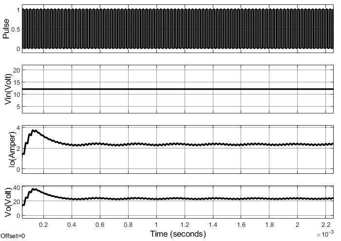
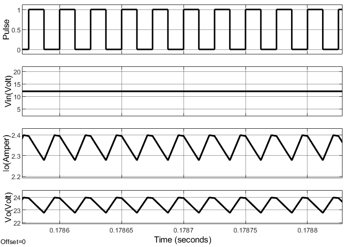
In Fig. 17, there are three parts first pulse generator, the output voltage, and the output current. All these parts show the characteristics of Performance criteria such as overshoot, undershoot, climb time, stability, as shown in the figure.
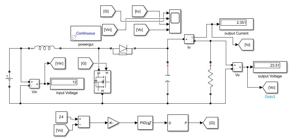
Second, the simulation model of the closed-loop system for the DC-DC boost converter as in Fig. 17 and the simulation results, as in Fig. 18 to Fig. 20. The output voltage is approximately 24 V at an input 12 V.
In the first simulation section there are two simulation model of dc-dc boost converter include, first modeling of open loop for DC-DC boost converter circuit at input source 12 V to output voltage at 24 V DC with 10Ω load as show in Fig. 13. Second, modeling of close loop for DC-DC buck converter circuit at input source 12 V to output voltage at
24 V DC with 10 Ω load as show in Fig. 17. Also, the simulation response for this converter as in Fig. 18 and
Fig. 19 that show pulse generator, input voltage, output current and voltage.
In Fig. 18, this figure includes four waves representing four quantities, one of which is the trigger pulse generated by the pulse generator, which controls the opening and closing intervals of the electronic switch. The second wave represents the input voltage from a DC source. The third and fourth waves represent the output voltage and current, which in turn represent the voltage and current of the resistive load connected to the converter's output.
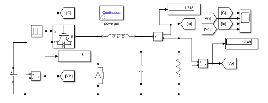
In the second simulation section there are two simulation model of dc-dc buck converter include, first modeling of open loop for DC-DC buck converter circuit at input source 48 V to output voltage at 18 V DC with 10Ω load as show in
Fig. 20. Also, the simulation response for this converter as in Fig. 21 to Fig. 23 that show pulse generator, input voltage, output current and voltage.
Second, modeling of a closed loop for DC-DC buck converter circuit at input source 48 V to output voltage at
18 V DC with 10 Ω load as shown in Fig. 24. Also, the simulation response for this converter is shown in Fig. 25 to Fig. 27, which show pulse generator, input voltage, output current, and voltage.
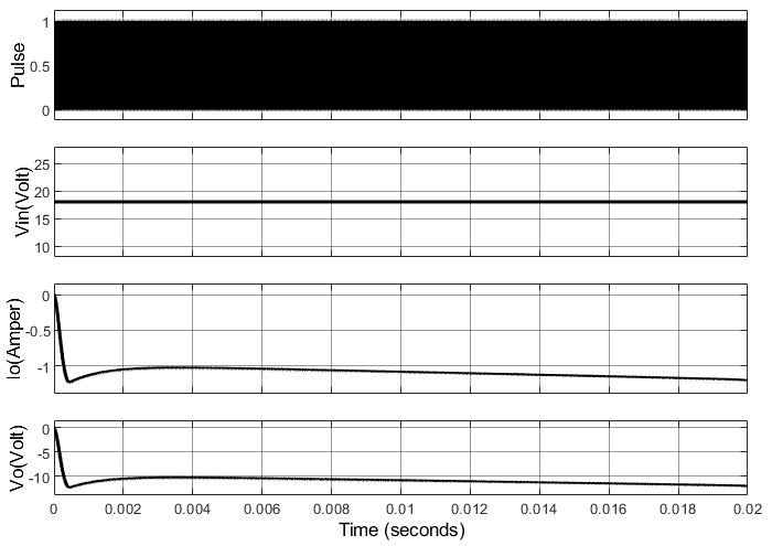
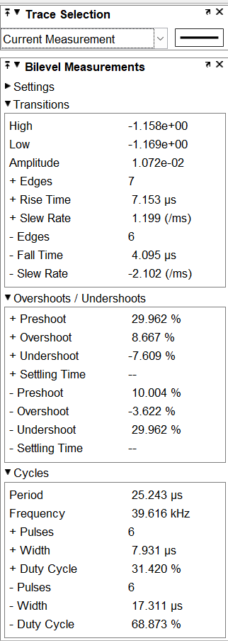
Fig. 20 shows the modeling of the open loop for the DC-DC buck converter circuit at an input source of 48V to an output voltage of 18 V DC with a 10 Ω load. Also, the simulation response for this converter, as in Fig. 21, includes a pulse generator, input and output voltage, with output current. Fig. 22 shows the response of the open loop for the DC-DC buck converter (0.0173-0.01775) seconds, which includes the pulse generator, input voltage, output current, and voltage. Fig. 23 shows the Trace Section pulse generator, Io & Vo, overshoot, undershoot, and rise time for the pulse generator, input and output voltage, with output current.
Fig. 24 shows the modeling of the closed loop for the
DC-DC buck converter circuit at an input source of 48 V to an output voltage of 18 V DC with a 10 Ω load. Also, the simulation response for this converter, as in voltage and current sensors, includes an input voltage (48 V), output voltage (18.1 V), and output current (1.81 A).
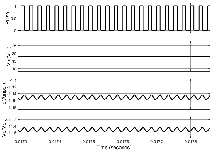
In the second simulation section, there are two simulation models of a DC-DC buck-boost converter, the first modeling open loop for the DC-DC buck-boost converter circuit at an input source of 18 V to an output voltage of -12V DC with a 10 Ω load, as shown in Fig. 28. Also, the simulation response for this converter is shown in Fig. 29 and Fig. 30, which show the pulse generator, input voltage, output current, and voltage.
Second, modeling of a closed loop for the DC-DC buck converter circuit at the input source -12 V to output voltage at 18 V DC with 10Ω load as shown in Fig. 31. Also, the simulation response for this converter is shown in Fig. 32 to Fig. 34, which shows the pulse generator, input voltage, output current, and voltage.
Discussion of open-loop system results: In the first step to obtain the system results, an input voltage sensor was connected to plot the input waveform, which was proposed to be a constant-value DC waveform over time for the operating period, as shown in Fig. 12, with a voltage of 12 volts.
Fig. 13 shows the input current waveform. Fig. 14 and
Fig. 15 show the output waves for the load voltage and current for the open-loop system, while Fig. 16 and Fig. 17 show the output waves for the load voltage and current for the closed-loop system.
A prototype was proposed, implemented, and mathematically represented, and theoretical calculations were performed to design simulation models according to the proposed specifications. The effectiveness of the closed-loop system for the boost converter was verified by increasing the supply voltage from 12 V to 24 V to meet the load requirements (10 Ω). The effectiveness of the closed-loop system for the buck converter was verified by reducing the supply voltage from 48 V to 18 V to meet the load requirements (10 Ω). The effectiveness of the buck-boost converter closed-loop system was verified by providing the required voltage to meet the load requirements (10 Ω). Based on the results, conclusions can be drawn, including the possibility of designing a boost converter used for many applications in various fields, characterized by high efficiency, high performance, and quality. Based on the results, conclusions can be drawn, including the possibility of designing a buck-boost converter used for many applications in various fields, characterized by high efficiency, high performance, and quality performance.
The use of control techniques has proven the possibility of improving the converter's performance under realistic conditions. Following the implementation, it was observed in the simulation that the system, operating under electronic switching control, could return to a stable state, thus achieving optimal performance. The converter's performance can be further developed and improved in future work by utilizing expert and intelligent systems, including fuzzy logic, genetic algorithms, neural networks, and others.
The proposed tests investigated the feasibility of designing an efficient system capable of providing the required output, specifically the specified voltage, to meet the load requirements. The converters used in this study can cover a wide range of applications due to their high efficiency and suitability for various uses, including powering electric vehicle motors, computer systems, electric elevator drives, and control systems, and more.
Salam Waley Shneen, Study, Design, Modeling, Simulation, and Control Analysis of DC-DC Power Converters